Hardware Update Logs
V1
First release
2017-6-1 public sale
Schematic diagram of V1
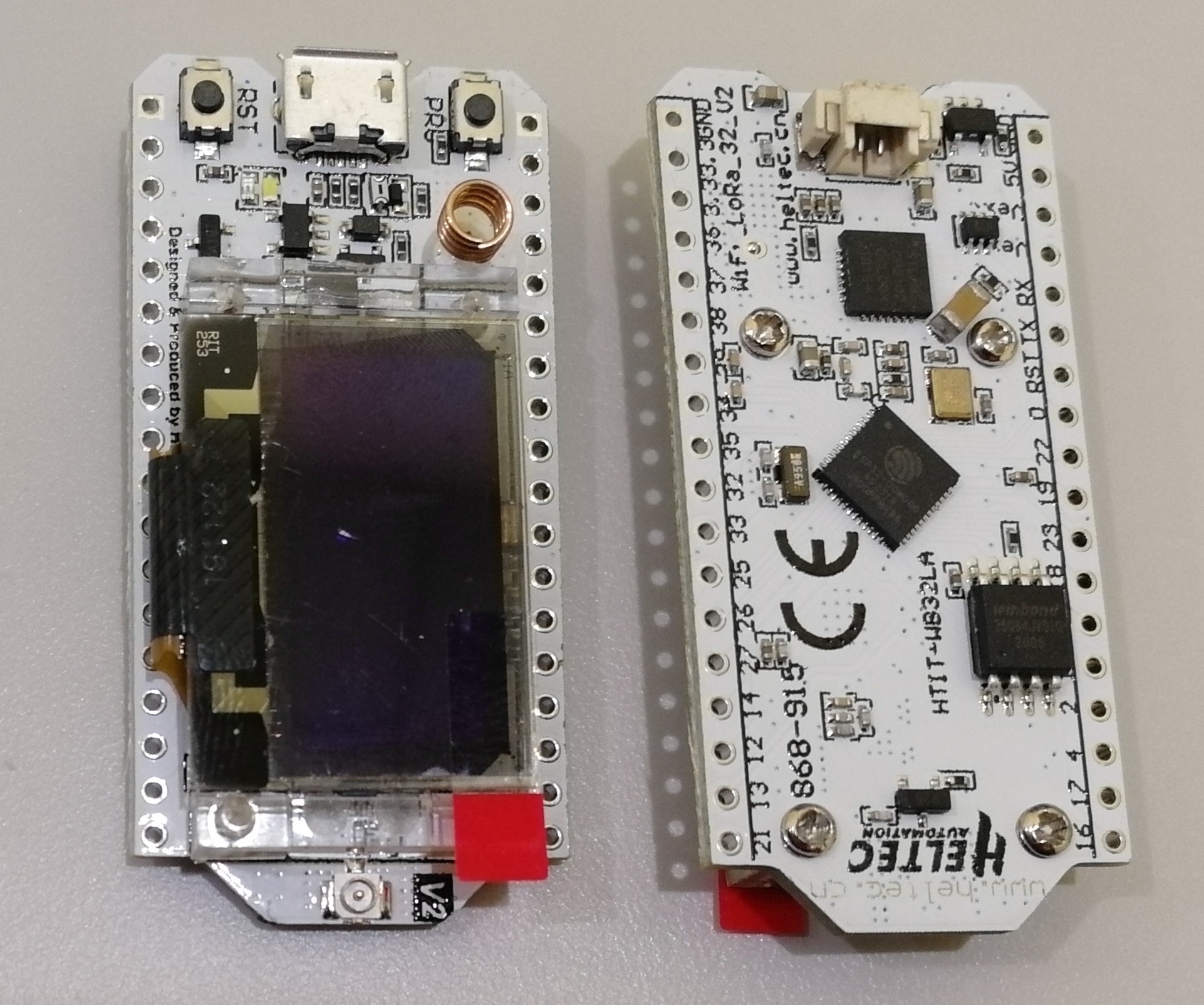
V2

2018-9-15 public sale
4MB (32M-bits) FLASH upgrade to 8MB (64M-bits) FLASH;
Use 40MHz HSE (V1 use 26MHz);
Basic low power design (800uA in deep sleep);
Add Vext power output pin, users can use this pin to drive some external device (sensor, motor etc.), when system need into deep sleep mode, Vext can be turn off.
This pin was controlled by GPIO21, for example:
Turn ON:
digitalWrite(21, LOW); Turn OFF:
digitalWrite(21, HIGH);Changed some pin connection:
Circuit optimization, system more stable;
Better power manage system design;
Better RF impendence matching.
Schematic diagram of V2
V2.1
2019-6-15 public sale
Change the RF switch from PE4259 to UPG2179, and change the RF part to the official recommended value;
Change the power detection pin from 13(ADC2: 4) to 37(ADC1: 1).
Schematic diagram of V2.1
V3
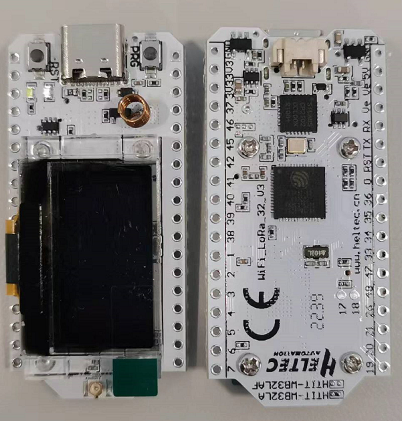
2022-09-15 public sale
MCU is changed from ESP32-D0WDQ6 to ESP32-S3FN8. Specific differences of MCU are shown in:https://products.espressif.com/#/product-comparison.
USB interface changed from Micro USB to Type-C.
LoRa chip changed from SX1276 to SX1262.
The LoRa crystal oscillator is upgraded to temperature compensated crystal oscillator.
The size, appearance, pin layout and power pins remain unchanged, but the GPIO sequence has changed. Please refer to Pinout diagram.
_V3.png)
V3.1
Remove the ideal diode part.
Increase the 2.4G RF and crystal distance.
Change the USB-Type-C port to support C to C.
V3.2
The new Schematic Diagram
Vext changed to LDO.
Modified the layout according to espressif’s suggestions for changes.
Modify the problem of easy adhesion of some parts.
The charging chip is changed to LGS4056H.
Modified voltage detection circuit, now need to pull up the ADC_Ctrl(GPIO 37).
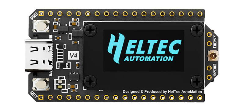
V4.0
MCU:
From ESP32-S3N8 to ESP32-S3R2
Flash has been upgraded from 8MB built-in to 16MB external, with the addition of 2M PSRAM.
Power:
Add SH1.25-2P solar energy interface.
Wireless performance:
LoRa transmission power upgraded from 21 ± 1dBm to 28 ± 1dBm.
2.4G antenna, upgraded from metal spring antenna to FPC antenna.
Peripheral Interface:
Cancel CP2102.
Add SH1.25-8Pin GNSS interface.
Pin expansion from 36Pin to 40Pin, providing more GPIO.
Process and Design:
The screen connection method has changed from welding to B2B interface, supporting free disassembly and assembly of the screen.
The pin process has changed from silver plating to gold plating, resulting in better conductivity and oxidation resistance.
There is a plastic screen stand as mechanical protection